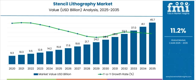
The Stencil Lithography Market is estimated to be valued at USD 15.8 billion in 2025 and is projected to reach USD 45.7 billion by 2035, registering a compound annual growth rate (CAGR) of 11.2% over the forecast period.
| Metric | Value |
|---|---|
| Stencil Lithography Market Estimated Value in (2025 E) | USD 15.8 billion |
| Stencil Lithography Market Forecast Value in (2035 F) | USD 45.7 billion |
| Forecast CAGR (2025 to 2035) | 11.2% |
The stencil lithography market is experiencing consistent expansion supported by rising demand for advanced nanofabrication techniques in electronics, chemical processing, and material sciences. The method is valued for its ability to pattern materials at the nanoscale without requiring complex photomasks, reducing production costs and enhancing flexibility in research and industrial applications.
Growing investments in semiconductor miniaturization and material engineering are further reinforcing adoption. The integration of stencil lithography in high precision manufacturing processes has also been accelerated by the increasing need for sustainable and efficient production technologies.
With advancements in process automation and alignment accuracy, stencil lithography continues to gain traction as a viable alternative for prototyping and niche fabrication needs. The future outlook is favorable as industries prioritize scalability, efficiency, and innovation in nanoscale patterning.
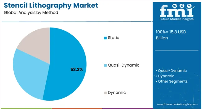
The static method segment is projected to hold 53.20% of total revenue by 2025 within the method category, making it the leading approach. Its dominance is linked to operational simplicity, lower setup requirements, and suitability for precise nanoscale deposition.
The method has been widely utilized in experimental setups and small scale manufacturing where accuracy and repeatability are critical. Static stencil lithography provides reliable control over material transfer, which is essential in semiconductor fabrication, electronics, and advanced material studies.
Its ability to support cost effective and reproducible outcomes has reinforced its preference over dynamic methods, positioning it as the most prominent segment.
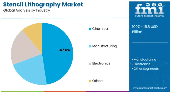
The chemical industry segment is expected to account for 47.60% of total market revenue by 2025 under the industry category, establishing it as the dominant application sector. This growth is being driven by the rising need for precise patterning in chemical synthesis, catalysis, and advanced material processing.
Stencil lithography enables efficient deposition of functional materials and supports innovation in nanoscale chemical engineering. Its application in creating patterned catalysts, sensors, and coatings has gained significant traction, supported by investments in R&D and industrial innovation.
As the chemical industry continues to focus on sustainability, efficiency, and precision, stencil lithography is anticipated to play a central role in enabling scalable and high performance processes.
More and more stencil lithography market participants from various areas are anticipated to fuel further market expansion. Moreover, throughout the study, the market is anticipated to be enhanced by rising expenditures made by notable vendors in product capabilities as well as business growth.
In growing countries like China and India, where substantial populations are combined with recent breakthroughs in a variety of industries, many industry participants perceive attractive prospects.
For example, Canon Inc. released the Lithography Plus1 solution architecture for semiconductor lithography equipment in September 2025. To increase support efficiency and suggest and put into place optimized system procedures, Canon incorporates its great amount of data and its more than 50 years of expertise in supporting semiconductor lithography systems.
Also, in June 2025, Samsung and ASML began to collaborate to create High-NA (high numerical aperture) ultraviolet (EUV) lithography equipment that will be marketed the following year. The next-generation High-NA EUV Lithography technology can etch finer circuits than prior EUV lithography equipment.
Stencil lithography happens to be an early technique that has been used to transfer patterns on different substrates. Currently, the stencil lithography technique is being applied to nano fabrication and micro-fabrication. This technique permits the wafer-scale transfer of nano-structures with the help of methods such as deposition, etching, and implantation.
In 1959, stencil lithography was first reported in a scientific journal as a micro-structuring technique by S. Gray and P. K. Weimer. Stencil lithography happens to be a shadow-mask technique which is primarily used for structuring surfaces at the nanometer and micrometer scales.
This technique helps in eliminating the processing steps that are usually involved in the standard lithography. Alternatively, stencils can be reused many times, which are entirely separated from the substrate and positioned by means of a manipulator. This offers cost effective pattern replication with the help of various materials onto different substrates.
Moreover, the potential of stencil lithography for a broad range of processes, materials, and applications is already being proved. One of the major applications for stencil lithography is the ability to construct arrays of structures with controlled dimensions on the nanometer scale specifically positioned on an appropriate surface.
Such capabilities would drive the demand for stencil lithography technology, in the coming years.
On the basis of modes, the stencil lithography market has been segmented into three types namely, static, quasi-dynamic, and dynamic. In the static mode, the stencil is lined up and fixed to a substrate. In quasi-dynamic mode, the stencil moves in relation to the substrate without breaching the vacuum.
Whereas, in the dynamic mode, the stencil moves relative to the substrate during deposition, letting the fabrication of patterns by changing the speed of the stencil while maintaining a constant deposition rate. Among the three modes, the dynamic mode happens to hold the largest share of the market and is also expected to grow at the highest rate, over the forecast period.
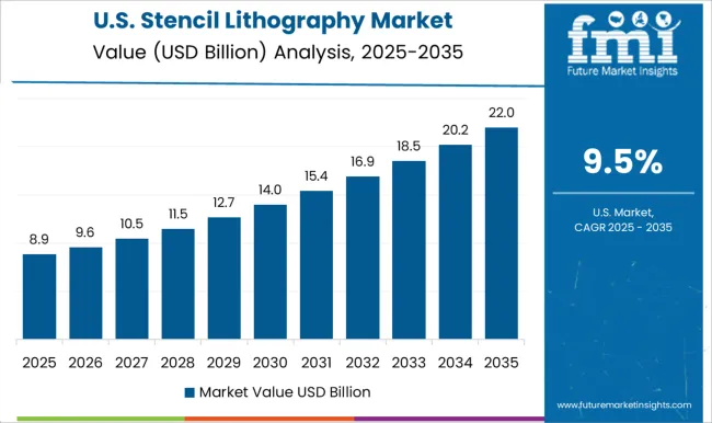
The USA happens to hold the largest share of the stencil lithography market in the North America region. Whereas, Canada would offer lucrative opportunities and is expected to grow at the highest CAGR over the forecast period. Moreover, the presence of established players in the stencil lithography happens to be one of the major factor contributing to the market growth in the North America region.
Furthermore, technological advancements in the field of lithography happens to be another major factor driving the demand and use-cases for stencil lithography techniques, in North America.
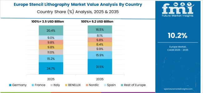
Major factors accelerating the growth of stencil lithography in European countries happen to be the rising demand for increased flexibility of patterning methods in engineering fields. Stencil lithography is a technique based on the standard of shadow masking a flux of molecules, atoms, or particles in order to modify the surface of a substrate.
The process of stencil lithography can accommodate a variety of methods such as etching, deposition, or ion implantation. With the rise in demand for nano and micro-fabrication, the demand for stencil lithography in countries like United Kingdom, Germany, France and others, is projected to grow over the forecast period.
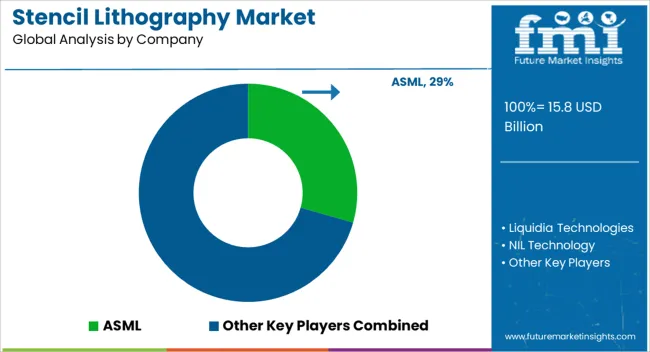
Some of the leading vendors offering stencil lithography services include
For instance, in July 2020, ASML announced innovations in lithography. The company’s holistic lithography incorporates a set of products that permits chipmakers in the market to develop, control, and optimize the process of production with the help of a nanometer logic and other nodes.
Other vendors in the market are adopting various key strategies in order to increase their customer base across the globe. They are also spending millions of dollars into research and development of products in order to fulfill the unmet needs of their customers for stencil lithography technology.
The report is a compilation of first-hand information, qualitative and quantitative assessment by industry analysts, inputs from industry experts and industry participants across the value chain. The report provides in-depth analysis of parent market trends, macro-economic indicators and governing factors along with market attractiveness as per segments.
The report also maps the qualitative impact of various market factors on market segments and geographies.
How big is the stencil lithography market in 2025?
The global stencil lithography market is estimated to be valued at USD 15.8 billion in 2025.
What will be the size of stencil lithography market in 2035?
The market size for the stencil lithography market is projected to reach USD 45.7 billion by 2035.
How much will be the stencil lithography market growth between 2025 and 2035?
The stencil lithography market is expected to grow at a 11.2% CAGR between 2025 and 2035.
What are the key product types in the stencil lithography market?
The key product types in stencil lithography market are static, quasi-dynamic and dynamic.
Which industry segment to contribute significant share in the stencil lithography market in 2025?
In terms of industry, chemical segment to command 47.6% share in the stencil lithography market in 2025.
Full Research Suite comprises of:
Market outlook & trends analysis
Interviews & case studies
Strategic recommendations
Vendor profiles & capabilities analysis
5-year forecasts
8 regions and 60+ country-level data splits
Market segment data splits
12 months of continuous data updates
DELIVERED AS:
PDF EXCEL ONLINE

Thank you!
You will receive an email from our Business Development Manager. Please be sure to check your SPAM/JUNK folder too.